Since carbon nanotubes have unique electrical properties, mechanical properties, excellent physical and chemical stability, and easy ink, it has become one of the ideal semiconductor materials for the printed thin film transistors, especially the printed flexible thin film transistors.
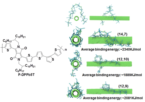
Recently, ZHAO Jianwen research group and MA Changqi research group from Printable Electronics Research Center of the Suzhou Institute of Nano-tech and Nano-bionics (SINANO) CAS worked together, designed and synthesized a series of new conjugated compounds (P-DPPb5T, 3T, 6T, 9T and 18T). P-DPPb5T, a new semiconducting copolymer was designed and synthesized with a special nonlinear structure and more condensed conjugation surfaces, which can separate large diameter semiconducting single-walled carbon nanotubes (sc-SWCNTs) from arc discharge SWCNTs according to their chiralities with high selectivity. With the sorted sc-SWCNTs ink, thin film transistors (TFTs) have been fabricated by aerosol jet printing. The TFTs displayed good uniformity, low operating voltage (±2 V) and subthreshold swing (SS) (122–161 mV dec−1), high effective mobility (up to 17.6–37.7 cm2 V−1 s−1) and high on/off ratio (104–107). With the printed TFTs, a better CMOS inverter was constructed. Relative research results were published on Nanoscale, 2016, 8, 4588-4598.

Figure1 Absorption spectra and PLE image of sorted SWCNT solutions, and electrical properties of printed SWCNT TFTs based on sorted sc-SWCNTs (Nanoscale, 2016, 8, 4588-4598.)

Figure 2 The cross-sectional and the horizontal views of the wrapping configurations of P-DPPb5T on SWCNTs with different chirality (Nanoscale, 2016, 8, 4588-4598.)
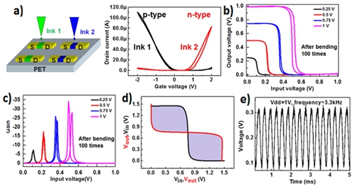
On the basis of the above work, by tuning the types of polymer-sorted semiconducting single-walled carbon nanotube (sc-SWCNT) inks ZHAO Jianwen research group found that P-type and n-type top-gate carbon nanotube thin-film transistors (TFTs) can be selectively and simultaneously fabricated on the same polyethylene terephthalate (PET) substrate. Both the p-type and n-type TFTs show good electrical properties with on/off ratio of ≈105, mobility of ≈15 cm2 V−1 s−1, and small hysteresis. Complementary metal oxide semiconductor (CMOS)-like logic gates and circuits based on as-prepared p-type and n-type TFTs have been achieved. Flexible CMOS-like inverters exhibit large noise margin of 84% at low voltage (1/2 Vdd = 1.5 V) and maximum voltage gain of 30 at Vdd of 1.5 V and low power consumption of 0.1 μW. A 3-stage ring oscillator has also been demonstrated on PET substrates and the oscillation frequency of 3.3 kHz at Vdd of 1 V is achieved. Relative research results were published on Small, 2016, DOI: 10.1002/smll.201600452.

Figure3 The schematic illustration of fabrication and electrical properties of n-type and p-type printed TFTs, performance of printed CMOS inverters on PET substrates and a 3-stage ring oscillator (Small, 2016, DOI: 10.1002/smll.201600452)

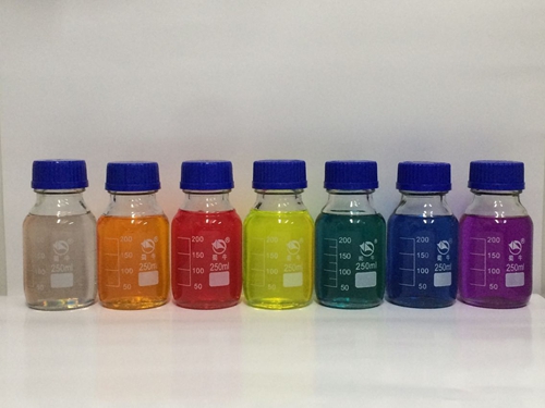
Figure 4 Printable sc-SWCNT inks
The above study was supported by National Natural Science Foundation of China, National Key Basic Research Program of China, Strategic Priority Research Program of the Chinese Academy of Sciences, Basic Research Program of Jiangsu Province and Suzhou Institute of Nano-tech and Nano-bionics.
(Information source: Nanjing branch of CAS)

