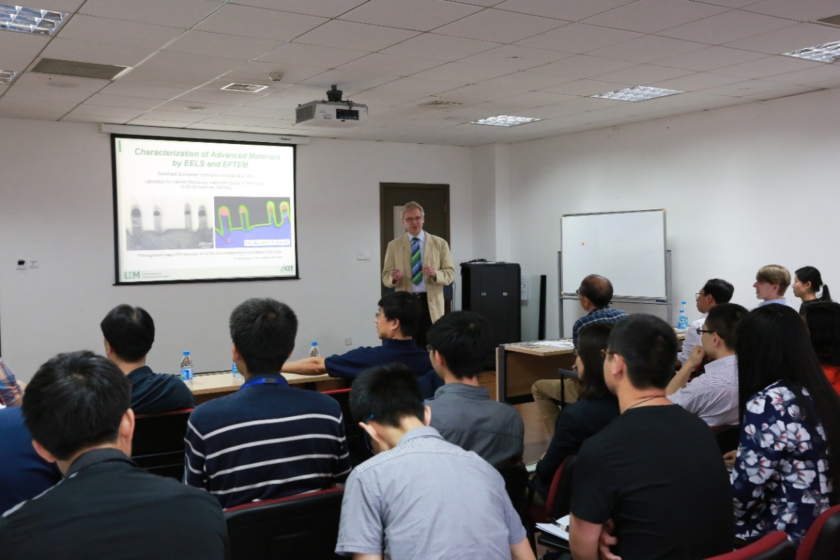
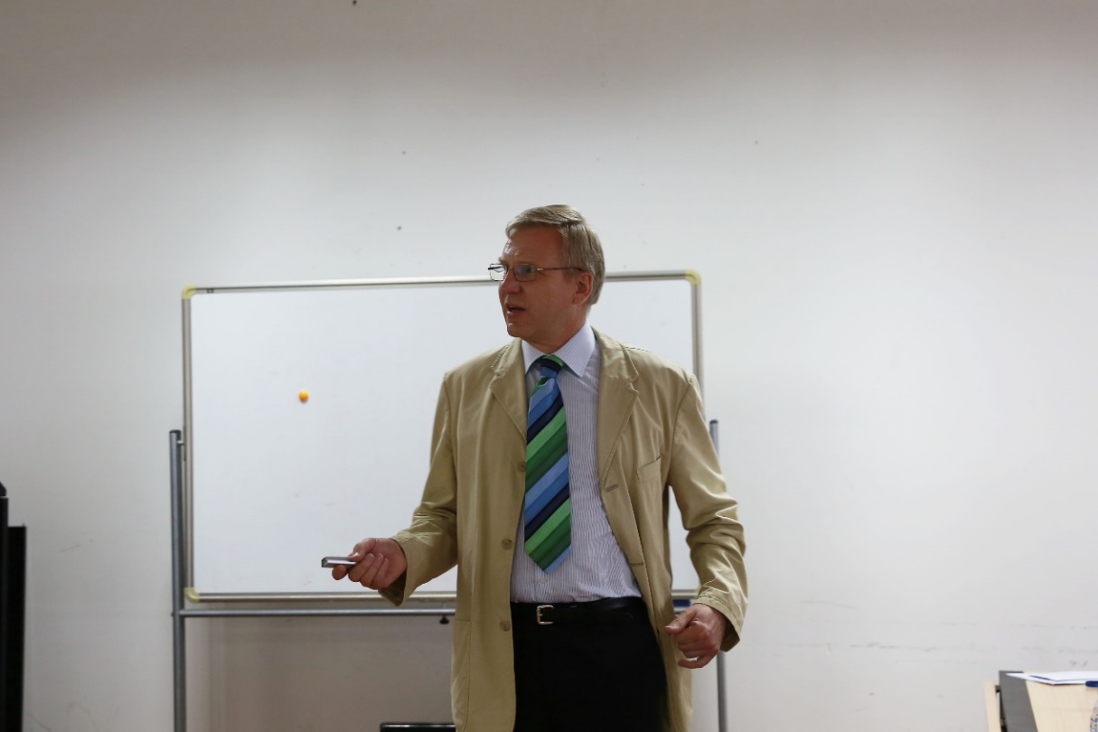
On June 8th, Dr. Reinhard Schneider from Karlsruhe Institute of Technology (KIT), Germany visited Suzhou Institute of Nano-tech & Nano-bionics, Chinese Academy of Sciences (SINANO). He was invited by Prof. Yuegang Zhang of i-Lab at SINANO. Dr. Schneider presented a lecture entitled “Characterization of advanced materials by EELS and EFTEM” during his visit to SINANO.
Although inelastic scattering of electrons passing through a thin sample in a transmission electron microscope (TEM) brings some disadvantages, i.e. leading to a blurring of image contrast, it also carries plenty of useful information, such as chemical composition of the sample, yielding the two widely applied techniques, Energy dispersive X-ray spectroscopy (EDXS) and Electron energy loss spectroscopy (EELS). Equipped with these two spectrometer, TEM is able to perform chemical analyses at nano-scale. EDXS is sensitive to elements with medium to high atomic number, while EELS is especially able to detect light elements at high efficiency. Therefore, these two techniques can be nicely combined. Further, the functionality of an EEL spectrometer can be extended to record two-dimensional element maps by the use of particular electron optics, which is energy-filtered TEM (EFTEM).
Dr. Schneider becomes a senior scientist in the Laboratory for electron microscopy (LEM) at KIT since January 2006. He is the head of TEM, and at present in charge of all the 5 TEMs in LEM, mainly the management of the Cs-corrected TITAN3 80-300 TEM (FEI). Except supervising master/doctor students in LEM, Dr. Schneider also undertakes a set of long-term service work concerning research and develop works in companies, such as Bosch GmbH.
At beginning of the lecture, Dr. Schneider gave a brief introduction on the physical fundamentals of inelastic electron scattering. Then he presented how powerful and how important of this EELS-EFTEM technique. Based on the results obtained from a broad range of advanced materials, he illustrated how to get information about the element composition as well as the chemical-bond state from combined EELS/EFTEM nanoanalytics. For example, a special specimen of Si, in which contains He bubbles, EELS could easily detect He although its atomic number as low as 2. It demonstrates that EELS is especially suitable for study light elements. EELS is also able to distinguish and quantify the sp2/sp3 hybridizations of C atoms in different C materials by the so-called energy loss near-edge fine structure (ELNES) technique. EFTEM studies on Si nanowires, metal-oxide nanoparticles, ZnO-based diluted magnetic semiconductors were also presented. Those results attracted much attention and Dr. Schneider had a lively discussion with the researchers and students after his lecture.


(Information Source: Suzhou Institute of Nano-Tech and Nano-Bionics, CAS)

