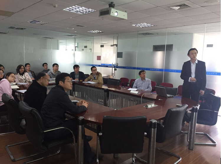
On April 28th, Invited by Professor Sun-an Ding, Prof. WANG Ke from Chiba University visited Nano-X and gave us an exciting report named “Molecular Beam Epitaxial Nitride Semiconductors: Epitaxy, Properties, and Solar Cell Applications".
III-Nitride semiconductors (InN, GaN, AlN and their alloys) offer wide direct bandgaps that can be tuned over the complete spectral range from deep ultraviolet (6.2 eV) to near infrared (0.7 eV). They have wide applications for optoelectronic and electronic devices. Historically MOCVD has played the major role in III-nitride devices. However, MBE (molecular beam epitaxy) has advantages in the case of high-In-content InGaN and InN, and when monolayer level control of sharp interfaces and layer thickness is required. The ultra high vacuum environment of a MBE system enables powerful in-situ diagnostic tools to understand the epitaxial growth mechanisms, and precisely control epitaxial processes. In this presentation, WANG Ke discussed the MBE growth of InN and InGaN thin layers and nano-columns. By using various in-situ monitoring tools, i.e., RHEED, laser reflection, and spectroscopic ellipsometry (SE), In adlayer assisted epitaxy of InGaN and InN, and the surface kinetics of In, Ga and Al adatoms have been thoroughly investigated. Special attentions have been paid to reduce the threading dislocations and residual electron density. P-type InN and InGaN across the entire alloy composition range have been achieved, despite of the notorious surface electron accumulation on high-In-content InGaN surfaces. Some important physical properties of InGaN will be discussed as well.
WANG Ke is an associate professor at Chiba University in Japan since 2013. His current research activities have involved growth, fabrication and characterization of III-V nitride semiconductor materials and devices. He received B. Sc degree from Nanjing University in 2000, the M.Phil degree from the University of Hong Kong in 2003, and the PhD degree from the University of Strathclyde, Glasgow, UK, in 2007. He joined Nanishi-Lab at Ritsumeikan University in Japan in 2008 and there received JSPS Fellowship. In 2013 he obtained the present academic position at Yoshikawa-Lab at Chiba University.
(Information source:Suzhou Institute of Nano-tech and Nano-bionics )
